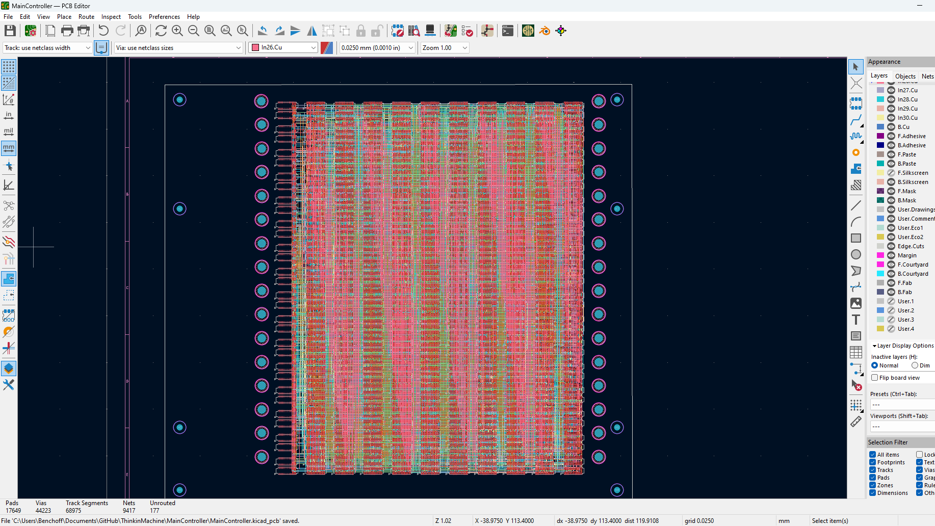
#kicad

14 posts · Last used Sep 17

This is a design I did a few days ago for @fafo@social.fa-fo.de, an I/V curve tracer for semiconductor testing. The idea here is to create a voltage ramp/sine across a potential semiconductor and trace the current flowing, against the voltage. If there are non-linear characteristics, you will see it in the resulting curve, it becomes curved or kinked. The board is basically just a specialized AFE for #analog-toolkit, an analog IO dev-board of mine. It's already with the manufacturer, lets see how it will turn out #electronics #kicad
76
11
16
0
Oops. I wish that when I had copied a symbol to make a new part in #KiCad, and then proceeded to forget to update the pinout, that I had at least used a symbol that had the pinout that 95% of the SOT23-5 buck converters on the market seem to use. But no, of course I copied the symbol with a pinout that only a few chips even used. And those are all asynchronous buck converters. 🙄 #electronics #pcb #screwup
1
3
0
0
I have never designed a PCB before, so, please tell me if this is okay. It's pretty simple: a STAC64 header (male pins) breaking out to discrete pads (which I will attach a short pigtail to that in turn attaches to a STAC64 female plug. There's a CAN H and CAN L breakout. TLDR: I'm meant to be working on a new review that requires installation of something that attaches to the CAN bus using.. wait for it... WIRE TAP SNAPS. 1) those fail and 2) I have had some bad experiences where I ended up breaking an entire cable. I'm not about to do that on an expensive truck I have a Digikey part order. I have the right diameter cables. I have a 3D printer, and I can make 2 sided PCBs on my CNC machine. The P-N is a direct correlation to the pin numbers of the STAC 64 connector. #KiCad #Circuits #DIY #Maker
3
4
0
0
Replying to
OK, this is total overkill, but I made my traces much larger, for increased success ;) Tell me it's workable?! #KiCad #Circuits #DIY #Maker
0
3
0
0
I would believe that #KiCAD has a perfectly rational way of doing things, and I just need to learn what that is, were it not for the objectively asinine way it handles board outlines, a thing that literally every PCB requires.
0
1
0
0
KiCAD Why why why? Wiring a schematic, the wires don't snap onto the nearest component terminal. Researching, it seems you have to have set the grid to the correct size and that your components have to be drawn to that too. The schematic is just an abstract representation of the circuit. Precise location in space has no meaning. Locking wires to the grid and therefore having them look like they've connected but not really is (to me) bloody stupid. I feel they should: A/ Snap to nearest terminal by default B/ Clearly highlight when they're loose-turn red, have a large coloured blob on the free end, something obvious. I'm sure I'm missing something. If anyone has been through this and can explain what I'm missing I'm keen to hear please :) #FirstWorldProblems #KiCAD
0
0
3
0
Intro post - many hashtags
Sensitive
0
0
2
0
Today #CERN released its #KiCad component library to the public. They are licensed CERN-OHL-P-2.0 Thank you OSPO ❤️ for getting this done. Originally the library is made in Altium and will also be maintained in Altium. The repo only contains files that have been automatically converted. It is a database library which contains only fully specified parts. There are lots of weird connectors. Have fun exploring.
84
1
85
0
New vid! #PCBs I made in 2025, part 1: LED charm ✨ https://www.instagram.com/reel/DTH1NuelDig Finally pulled together a prototype with this little board – one of my new #Charmware set, reviving the series of modular tech #jewelry bits I started back in 2018. Been dreaming of assembling these with elytra and bike-leather, and the day finally came... The board still needs some tweaks (smaller switch etc.), but with my fixed-up #KiCad workflow, those will be a snap. 😸 // #Maker #LEDs #WearableTech
78
12
25
0